USER'S VOICE
利用者の声
ユーザーレポート
サステナブルテクノロジー研究所
解析技術センター
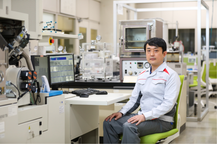
佐々木 宏和氏
当社は情報通信、自動車部品、エレクトロニクス製品を展開し、多くの製品を社会に提供しています。新製品開発において目的とする性能を発揮するには、使用する材料の構造や機能といった特性の理解が大切です。半導体レーザーと超電導線材の開発では東京大学の収差補正走査透過型電子顕微鏡(STEM)を使用しました。
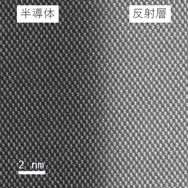
半導体レーザーは通信容量の増加に伴い世界的需要が増え、当社では光通信用の光源、長距離通信の増幅器を開発しています。半導体レーザーでは、光を反射する端面保護層を原子レベルの精度で作製する必要があります。適切に反射する層の形成を目指しSTEMで観察して試行錯誤を繰り返し、高出力半導体レーザーの開発に成功しました。
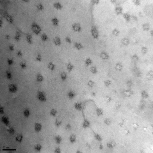
超電導線材は、高磁場を発生する超電導コイルなどへの応用が期待されます。超電導線材をコイルにし、強磁場を発生させると、超電導の中で磁場が量子化し超電導状態が保てなくなります。そこで、磁束量子の動きを止めるバリウムとジルコニウムの酸化物でできた人工ピン(数nm)を開発するため、STEMを利用し、人工ピンの適切なサイズを導き出し、機能向上につなげました。超電導コイルは、安全性が高くCO2 排出量が少ない核融合発電施設や高精度な画像診断が可能なMRIで使われることが想定され、今後の需要拡大が期待されます。
当社における多様な製品に対応するには、多くの高度解析装置が不可欠ですが、一企業が全てを所有することは難しいと言えます。
日本の企業が国際社会との競争力を失わないためには、ものづくりにおける信頼性を確保しなければなりません。それがベースとなってこそ、新たなイノベーションが生まれると思っています。設備機器や基礎技術が、国内にそろっていることが非常に大事で、大学と企業が力を合わせ、互いに有益な価値を生み出すことができれば得られるものは多いと言えます。高額な設備機器は、共有財産として使わせてもらうことで、その分の費用を開発に回すことができ、日本の産業の競争力を高めることにつながると思っています。
(ナノテクノロジプラットフォームユーザーレポート CASE03)