Focused ion beam scanning electron microscope complex system
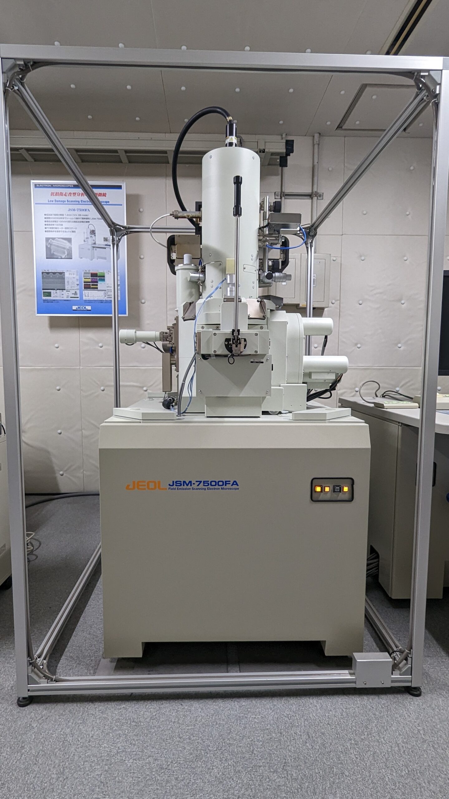
Low damage scanning analytical electron microscope (JSM-7500FA)
| Acceleration voltage | ~30kV |
|---|---|
| Electron gun | cold cathode field emission electron gun |
| image resolution | ~1.0nm(15kV) ~1.4nm(1kV) |
| statue type | Secondary electron image Backscattered electron image |
| Detector | Lower detector Backscattered electron detector |
| Others | GB (gentle beam) function available |
The use of a cold cathode field emission electron gun enables high resolution even at low acceleration voltages, making it suitable for observing specimens that are sensitive to electron beams.
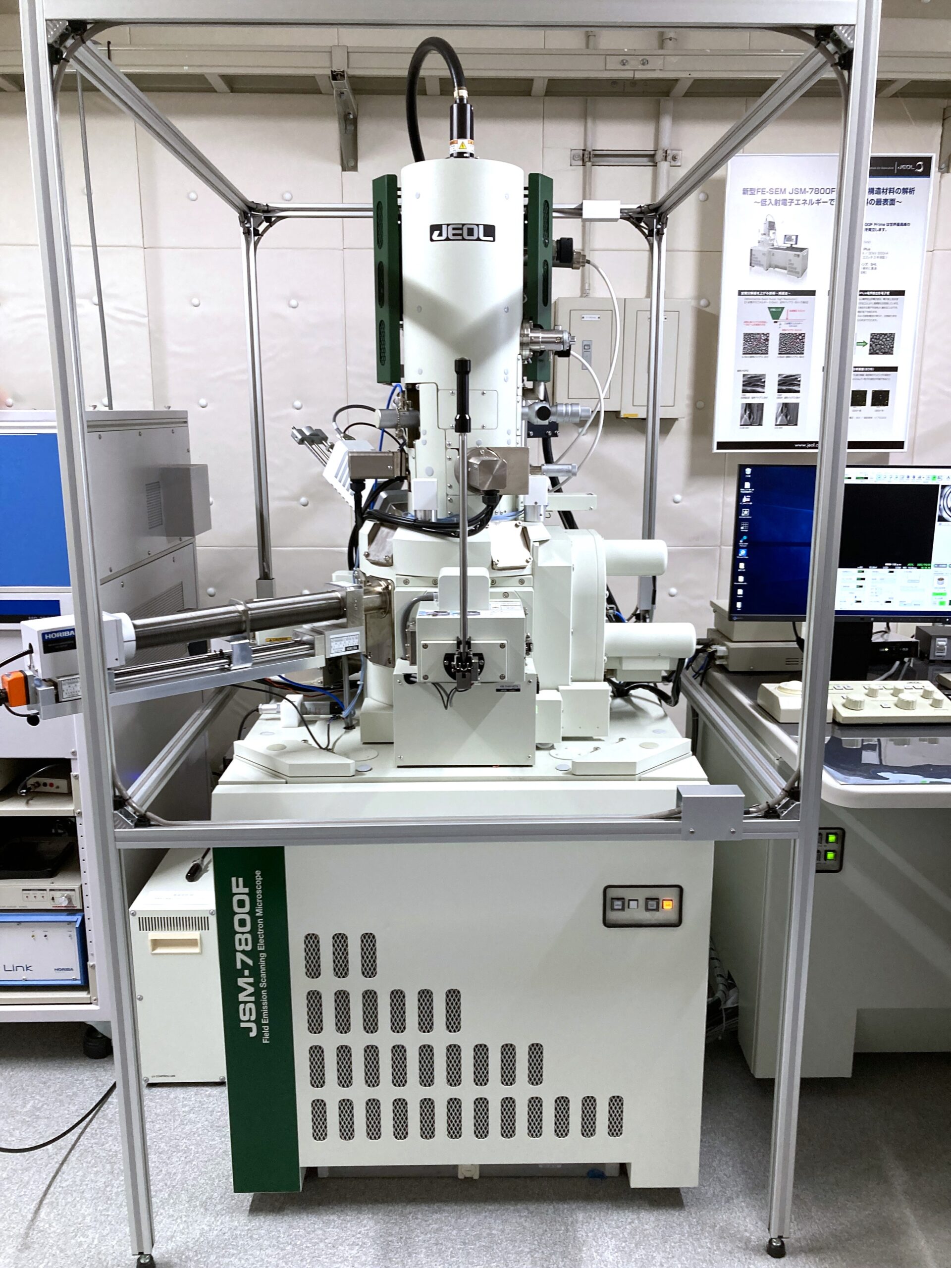
High resolution scanning analytical electron microscope (JSM-7800F-PRIME)
| Acceleration voltage | ~30kV |
|---|---|
| Electron gun | Schottky electron gun |
| image resolution | ~0.7nm(15kV) ~3.0nm(100V) |
| statue type | Secondary electron image Backscattered electron image |
| Detector | Lower detector upper detector Backscattered electron detector EDS (JEOL JED-2300) CL (HORIBA MP-32S) |
| Others | GB (gentle beam) function available |
Employing an in-lens Schottky field emission electron gun, this instrument enables stable analysis at high resolution and high irradiation current.
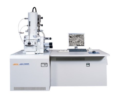
High resolution scanning electron microscope (JSM-7000F (EBSD))
| Acceleration voltage | ~30kV |
|---|---|
| Electron gun | In-lens shot - field emission type |
| image resolution | ~1.2nm(30kV) |
| statue type | Secondary electron image Backscattered electron image |
| Detector | Lower detector Backscattered electron detector EBSD |
In addition to enabling high-resolution observation of the surface morphology of various samples, crystal orientation analysis by EBSD can be performed.
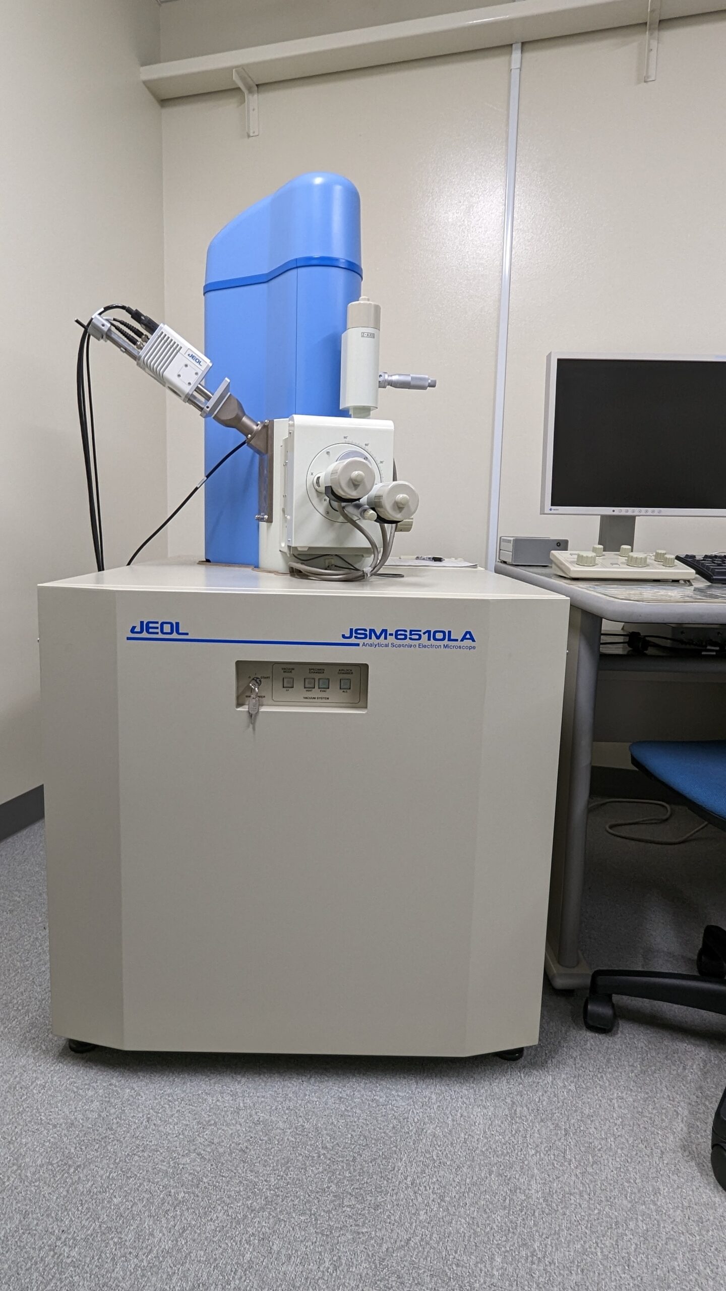
Low vacuum scanning electron microscope (JSM-6510LA)
| Acceleration voltage | ~30kV |
|---|---|
| Electron gun | thermal electron gun |
| image resolution | ~3.0nm(30kV) ~15.0nm(1kV) |
| Air pressure inside the sample chamber | 10 to 270Pa |
Observation is possible in a low-vacuum environment, and samples that cannot be subjected to conductive treatment can also be observed.
Focused ion/electron beam combined beam processing and observation device (JIB-PS500i)
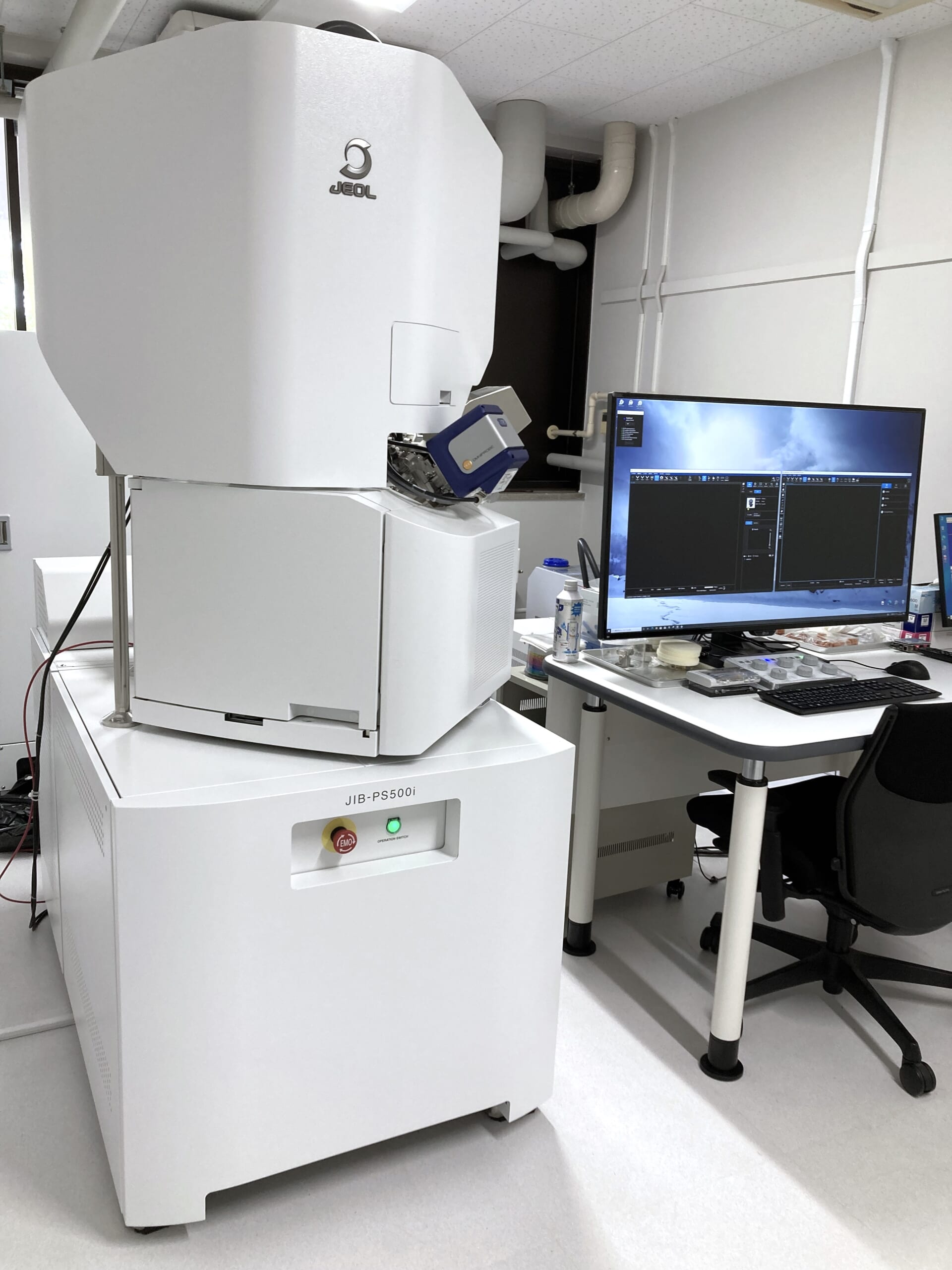
JEOL Ltd.
| FIB (Focused Ion Beam) | ・Ion source: Ga liquid metal ion source ・Acceleration voltage: 0.5 to 30kV ・Magnification: ×50 to ×300,000 ・Ion beam processing shape: rectangle, circle, polygon, line, spot, bitmap shape |
|---|---|
| SEM (electron beam) | ・Acceleration voltage: 0.01 to 30kV ・Magnification: ×20 to ×1,000,000 ・Image resolution: 0.7nm (acceleration voltage 15kV), 1.0nm (acceleration voltage 1kV) ・Detector: Secondary electron detector (SED), upper electron detector (UED), in-lens backscattered electron detector (iBED), retractable backscattered electron detector (RBED) |
・ Equipped with a high-resolution FE-SEM, it is possible to create pinpoint cross sections.
・ FIB processing status can be monitored in real time using high-resolution SEM
- Equipped with an in-lens thermal electron gun, enabling stable and high-speed analysis with a maximum current of 500nA.
・STEM observation possible (BF,HAADF)
Sample preparation device for electron microscope FIB XVision200TB (using FIB-SEM)
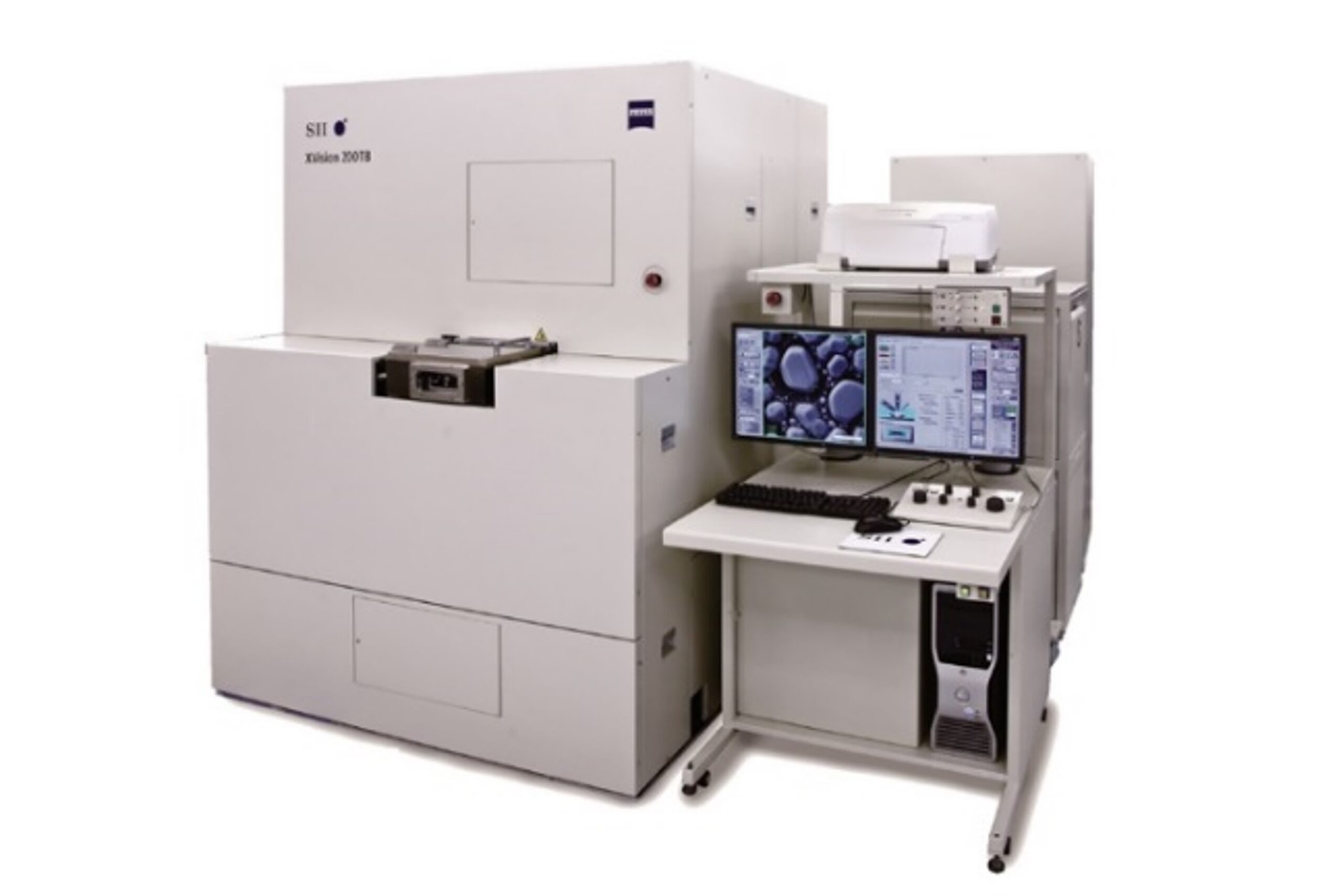
XVision200TB (Hitachi High Technologies)
| FIB resolution | 4nm@30kV (Accelerating voltage: 1-30kV) |
|---|---|
| SEM resolution | 3nm@5kV (Accelerating voltage: 1-30kV) |
| Ar ion gun | Accelerating voltage: 1 kV |
| sample stage | Supports up to 8 inches |
TEM sample preparation and cross-sectional observation (Cut&See)