Scanning Transmission Electron Microscope/Transmission Electron Microscope
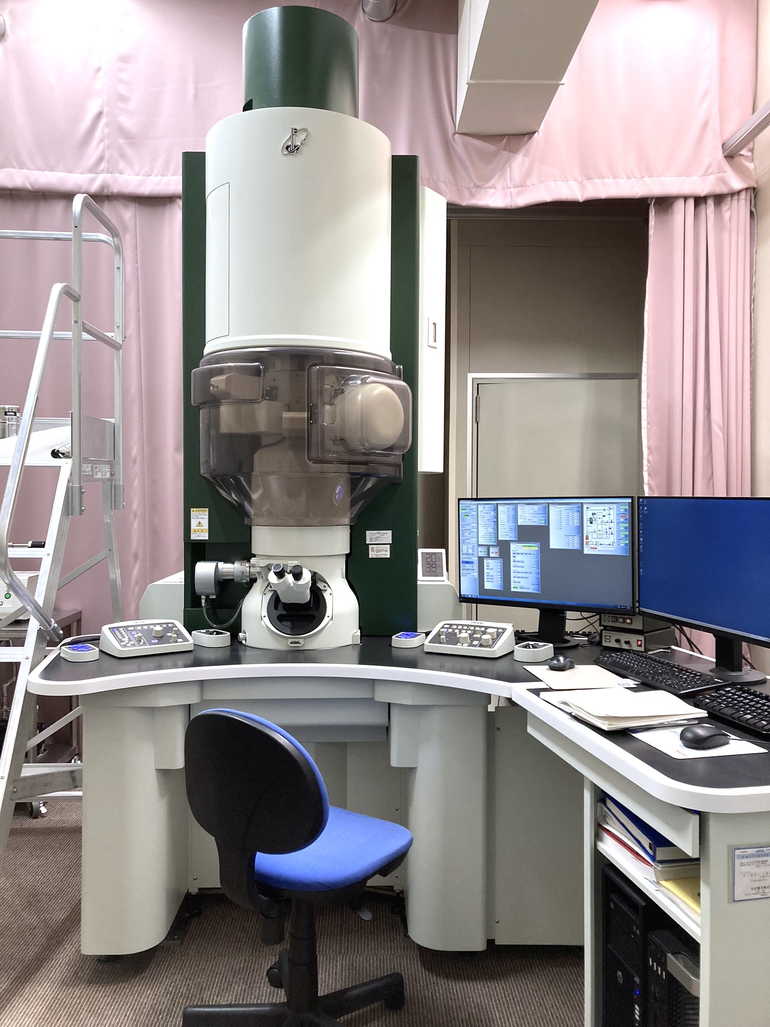
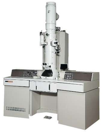
Atomic resolution scanning transmission electron microscope (NEO ARM) with low accelerating voltage
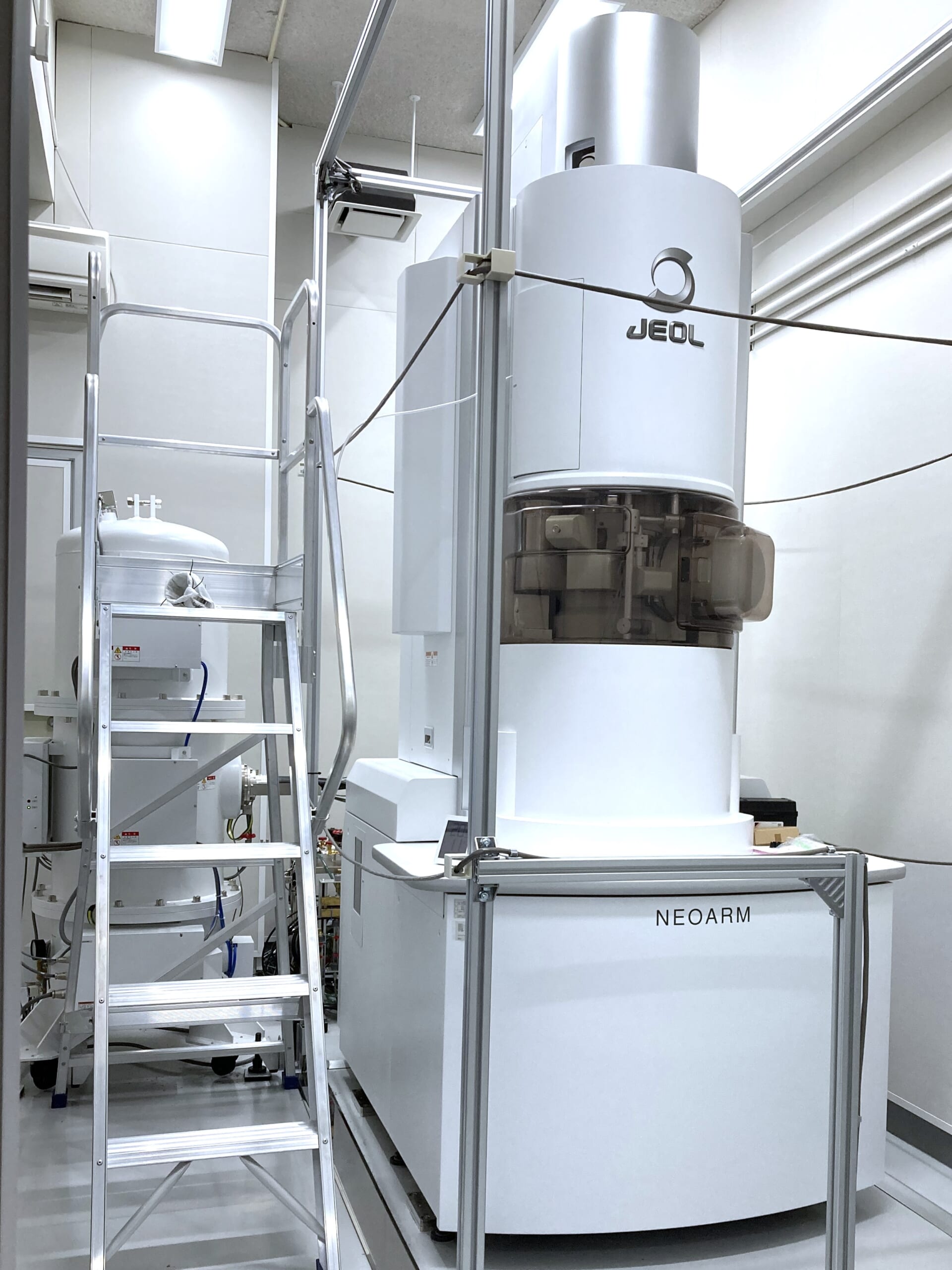
JEM-ARM200CF / JEOL
| Acceleration voltage | 30 - 200kV |
|---|---|
| resolution | 0.071 nm (200 kV), 0.11 nm (60 kV) |
| Analysis function | EDS, EELS |
| Features | cold cathode field emission electron gun Aberration corrector (probe correction) Remote control available |
Equipped with two high-sensitivity semiconductor X-ray detectors.Elemental analysis of each atomic column of crystalline materials with high spatial resolution is possible.
Scanning transmission electron microscope for light elements JEM-ARM200F ColdFE
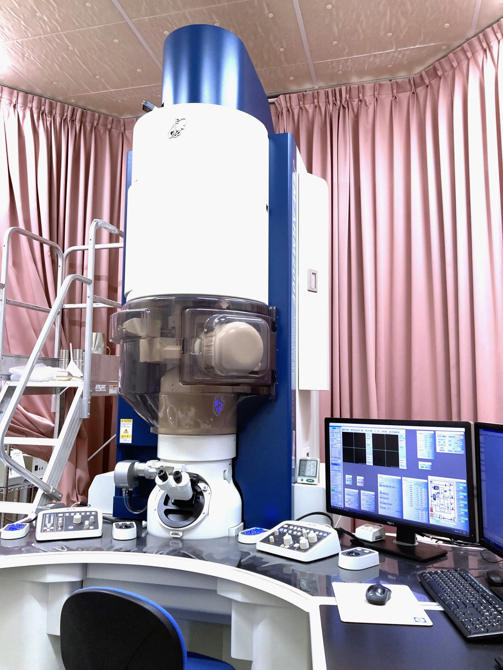
JEM-ARM200F ColdFE
| Acceleration voltage | 200kV/120kV |
|---|---|
| resolution | Scanning transmission image (using an annular dark field detector, acceleration voltage 200 kV) 0.08 nm |
| magnification | Scanning transmission image: 200 to 150,000,000 times / Transmission microscope image: 50 to 2,000,000 times |
| Aberration corrector | Irradiation system spherical aberration corrector built-in |
| Detector | Energy dispersive X-ray spectrometer (EDS), electron beam energy loss spectrometer (EELS), image detector for light elements, CCD detector (2k x 2k) |
Equipped with an illumination system spherical aberration corrector as standard, and by maximizing mechanical and electrical stability, it achieves the world's highest scanning transmission image (STEM-HAADF) resolution of 0.08 nm.
Ultra-high resolution transmission electron microscope JEM-ARM200F ColdFE
JEM-ARM200F Cold FE (Cs-HRTEM)
| Acceleration voltage | 200kV/120kV/100kV/80kV/60kV |
|---|---|
| resolution | Particle image transmission microscope resolution 0.10 nm (accelerating voltage 200 kV) |
| magnification | Scanning transmission image: 200 to 150,000,000 times / Transmission microscope image: 50 to 2,000,000 times |
| Aberration corrector | Imaging System Spherical Aberration Corrector |
| Detector | CCD camera, CMOS camera |
A transmission microscope image (TEM) resolution of 0.11 nm is achieved by installing an imaging system spherical aberration corrector.
Environmentally friendly ultra-high resolution electron microscope JEM-ARM200F ColdFE (STEM Double SDD)
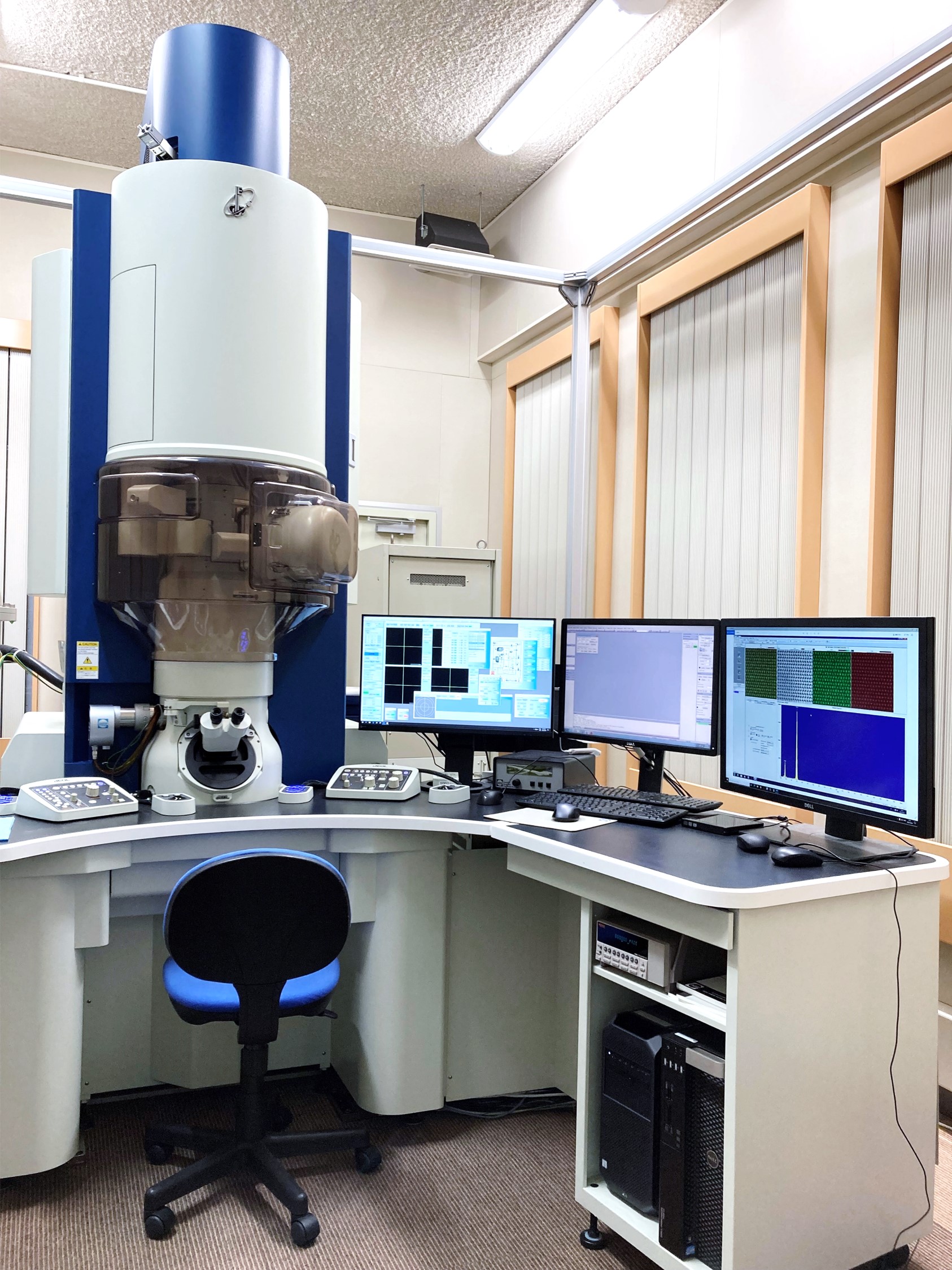
Made by JEOL
| Acceleration voltage | 200kV, 80kV |
|---|---|
| resolution | TEM lattice image 0.10nm TEM particle image 0.23nm STEM bright field grating image 0.136nm STEM dark field grating image 0.10nm |
| magnification | TEM image 50 to 2,000,000 times STEM image 200 to 150,000,000 times |
| Aberration corrector | Irradiation system spherical aberration corrector built-in |
| Detector | Energy dispersive X-ray spectrometer (SDD x 2) Electron Energy Loss Spectrometer (EELS) Image detector for light elements CCD detector (2k×2k, 4k×2k) |
| sample holder | Sample 2-axis tilt holder High temperature heating electric holder Air non-exposed holder |
Equipped with two high-sensitivity semiconductor X-ray detectors.Elemental analysis of each atomic column of crystalline materials with high spatial resolution is possible.
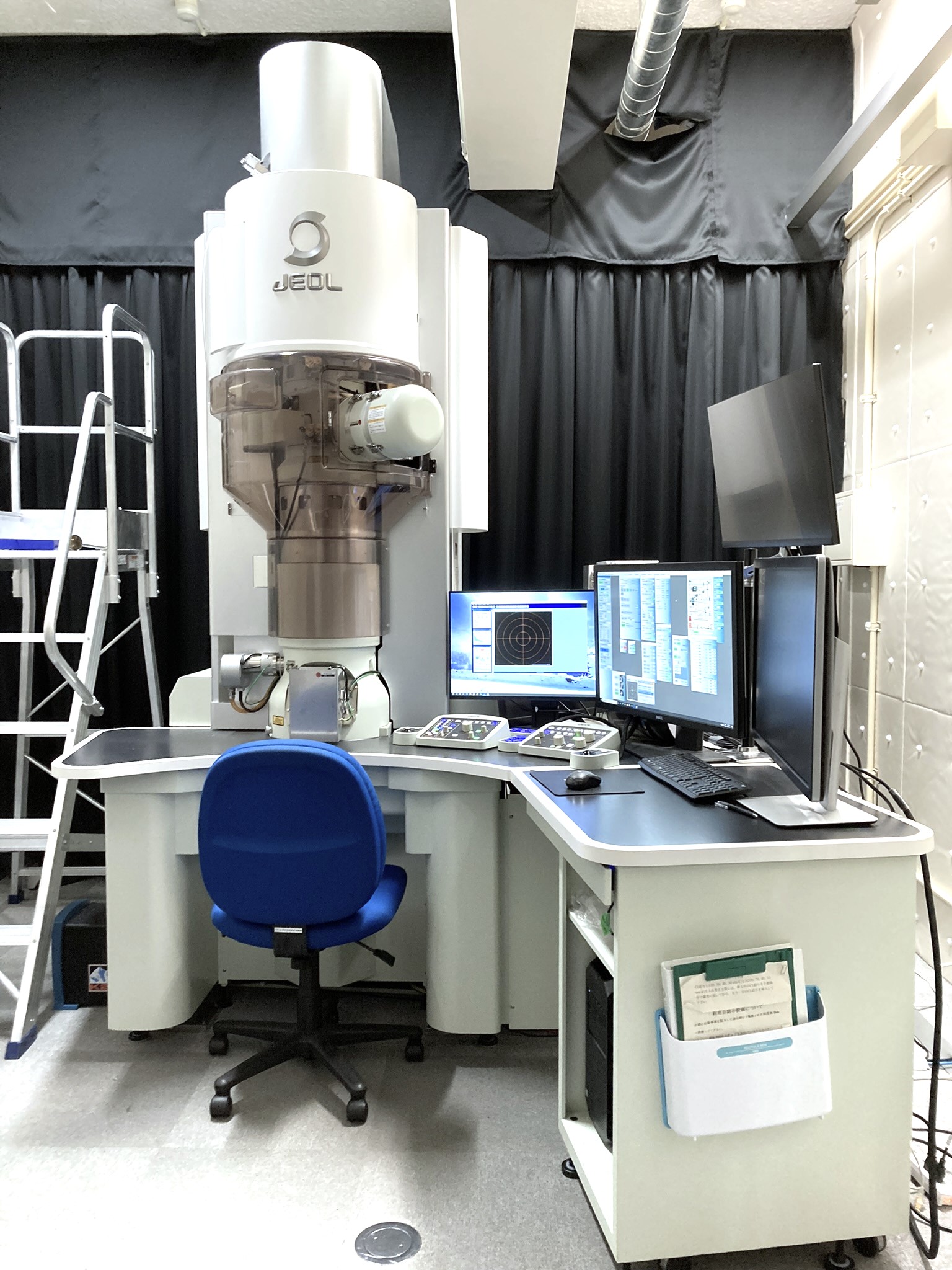
Atomic resolution elemental mapping structure analyzer JEM-ARM200F Thermal FE (STEM SDD)
JEM-ARM200F Thermal FE STEM / JEOL
| resolution | STEM bright field grating image 0.136nm STEM dark field grating image 0.082nm TEM lattice image 0.10nm TEM particle image 0.19nm |
|---|---|
| magnification | STEM image 200 to 150,000,000 times TEM image 50 to 2,000,000 times |
| Aberration corrector | Irradiation system spherical aberration corrector built-in |
| Detector | Energy dispersive X-ray spectrometer (SDD) Electron Energy Loss Spectrometer (EELS) Image detector for light elements CCD detector (2k×2k, 4k×2k) |
It has high image resolution and is useful for visualization of light element column positions, local structural analysis of lattice defects, and elemental mapping.
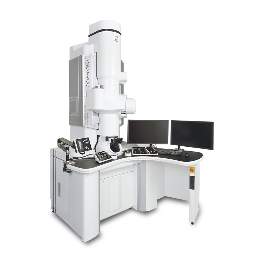
Multifunctional field emission transmission electron microscope JEM-F200
Transmission/scanning analytical electron microscope (TEM/STEM) JEM-2800
JEM-2800F made by JEOL
| Acceleration voltage | 100kV, 200kV |
|---|---|
| CCD camera | Gatan Orius (for TEM observation) Hamamatsu Photonics (for electron beam diffraction) |
| EDS | Made in Oxford |
| EELS | Gatan Enfina1000 |
High resolution analytical electron microscope (JEM-2010F)
JEM-2010F / JEOL
| Acceleration voltage | 80, 100, 120, 160, 200kV |
|---|---|
| electron beam source | Thermal field emission type |
| resolution | 0.192 nm (particle image) |
| Detector | EDS, CCD camera and sheet film available |
Easy-to-use standard analytical and high-resolution transmission electron microscope.
High contrast transmission electron microscope (JEM-2010HC)
JEM-2010HC / JEOL
| Acceleration voltage | 80, 100, 120, 160, 200kV |
|---|---|
| electron beam source | Single crystal LaB6 filament |
| Detector | EDS, CCD camera and sheet film available |
As a standard transmission electron microscope that is easy to operate, it has high-contrast specifications that facilitate morphological observation, shape observation, lattice defect observation, long camera length, and lattice defect analysis such as g and b analysis.
Cryo-transmission electron microscope JEM-2100F
Made by JEOL
| Acceleration voltage | 200kV, 120kV |
|---|---|
| Electron gun | Schottky type FE |
| Point resolution | 0.31 nm |
| Detector | EDS EELS CCD (4k×4k, 1k×1k) |
| sample holder | Cryotransfer holder for cryogenic observation tomography holder Sample 2-axis tilt holder |
It can be used for observation of biological samples, tissue sections, soft materials such as organic materials, low-temperature frozen sample observation, tomography, structural analysis, and elemental analysis.
*This TEM is used when preparing ice-embedded samples using Leica EM GP (automatic immersion freezing device) and using a cryo-transfer holder.
Transmission scanning electron microscope (JEM-2100F)
Made by JEOL
| Acceleration voltage | 200kV, 120kV |
|---|---|
| Electron gun | Schottky type FE |
| Point resolution | 0.31 nm |
| Detector | EDS EELS CCD (4k×4k, 1k×1k) |
| sample holder | Cryotransfer holder for cryogenic observation tomography holder Sample 2-axis tilt holder |
It can be used for observation of biological samples, tissue sections, soft materials such as organic materials, low-temperature frozen sample observation, tomography, structural analysis, and elemental analysis.
*The equipment is the same as the cryo-TEM above.Use this device if you are not performing low-temperature observation.
High-contrast electron microscope for organic materials (Bio-TEM JEM-1400)
JEM-1400 made by JEOL
| Acceleration voltage | 80-120kV |
|---|---|
| resolution | 0.38 nm (particle image) |
| Others | Autofocus function / automatic montage function (automatic stitching and automatic contrast correction, 5 million pixels in total for 5 vertical x 2500 horizontal images) |
Observation of high-contrast TEM images, which is essential for observing biological materials and macromolecular materials, is possible.The automatic montage function enables large-area observation and ultra-high-speed screening of biological samples while maintaining resolution.This TEM has an autofocus function and is easy to use even for beginners.
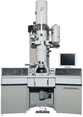
Atomic Direct View Ultra-High Voltage Electron Microscope (JEM-ARM1250)
JEM-ARM1250 / JEOL
| Acceleration voltage | 100, 150, 200, 250, 300, 350, 400kV |
|---|---|
| electron beam source | Single crystal LaB6 filament |
| resolution | 0.155 nm (particle image) |
| image recording | Sheet film and imaging plate (25 μm/pixel) |
Observation of thick samples is possible with high acceleration voltage.